
ASU gets $2M federal grant to develop water reuse tech for semiconductor manufacturing
As part of the project, ASU's Macro Technology Works in Tempe will test and certify new water treatment technology, creating the data needed for the industry to adopt water-saving solutions.

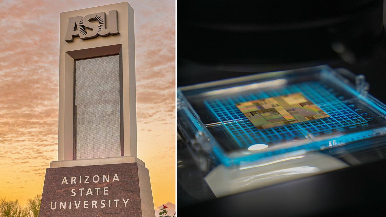
Arizona State University received more than $2 million in federal funding to develop and test water reuse technology for semiconductor manufacturing, officials announced Monday. (Photos via ASU on Facebook and Walid Berrazeg/Sopa Images/Light Rocket via Getty Images)
(Photos via ASU on Facebook and Walid Berrazeg/Sopa Images/Light Rocket via Getty Images)
Arizona State University received more than $2 million in federal funding to develop and test water reuse technology for semiconductor manufacturing, officials announced Monday.
The National Institute of Standards and Technology money was secured by U.S. Reps Greg Stanton and Yassamin Ansari and U.S. Sens Mark Kelly and Ruben Gallego.
As part of the project, ASU’s Macro Technology Works in Tempe will test and certify new water treatment technology, creating the data needed for the industry to adopt water-saving solutions.
“Arizona is proving that you can lead the nation in semiconductor manufacturing and be a responsible steward of every drop of water,” Stanton said in a news release. “This investment puts ASU’s researchers to work on exactly the right challenge: making sure the industry driving our economic future can grow without straining the water resources our communities depend on. That’s how we keep chip production strong and sustainable right here in Arizona.”
The university will use two phases to advance technology that is in the early stage of research to a point where it is ready for commercial use.
The first will develop and integrate fledgling treatment technology into a mobile, pilot-scale testing environment. The second will validate them at the Tempe facility using manufacturing-representative conditions.
Additionally, there will be quarterly reviews by stakeholders to decide what technology goes to the pilot-scale testing environment, where researchers quantify water savings, operational benefits and cost reductions.
“ASU looks forward to putting this federal investment to work advancing technologies that can help semiconductor manufacturers use water more efficiently and strengthen the resilience of chip production in Arizona,” ASU President Michael Crow said. “By developing and testing promising water reuse technologies in a semiconductor manufacturing environment, ASU can help advance these solutions for commercial use.”
Related
 Upper Verde River on verge of earning state’s highest water quality protection level
 Woman running 2,000 miles in 100 days to sound alarm about Colorado River water crisis
 Water expected to be restored to Grand Canyon’s South Rim in weeks following flash flood
 Grand Canyon shuts off potable water for visitors at South Rim in conservation effort
 Residents push for special election to designate Arizona’s McMullen Valley as AMA
 Upper Basin on verge of first-ever Colorado River Compact breach, CAP president warns

Comments
0 Comments